
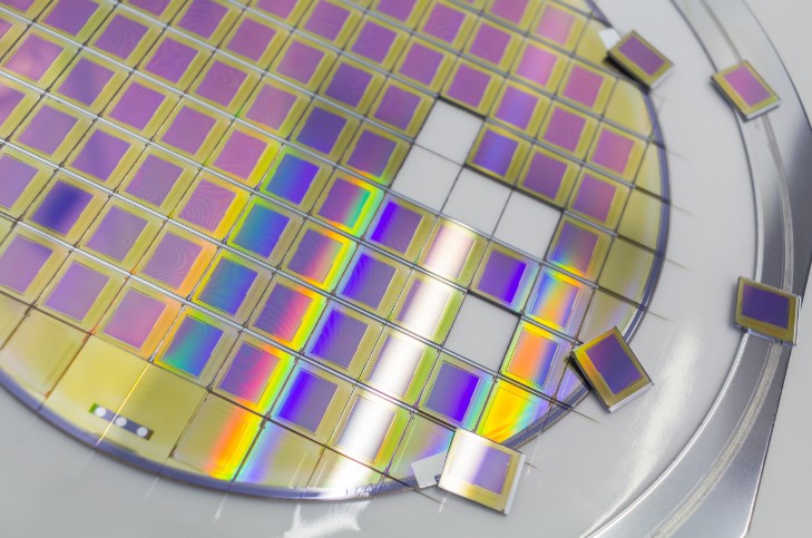
Wafer dicing is a critical step in the semiconductor manufacturing process that involves cutting a semiconductor wafer into individual chips or dies. Here are some facts about the wafer dicing process:
Purpose:
The primary purpose of wafer dicing is to separate the individual integrated circuits (ICs) or microchips that have been fabricated on a semiconductor wafer. This allows for the packaging and testing of these individual chips.
Methods:
There are several methods for wafer dicing, including mechanical sawing, laser cutting, and chemical etching. The choice of method depends on factors such as the material of the wafer and the desired precision of the cut.
Mechanical Sawing:
Mechanical sawing is a common dicing method. It uses a diamond-tipped saw blade to cut through the wafer. This method is precise and well-suited for most materials but generates some waste in the form of sawdust.
Laser Cutting:
Laser dicing uses a high-energy laser beam to ablate and cut through the wafer. It is a non-contact method, which reduces the risk of contamination and is suitable for cutting fragile or brittle materials.
Chemical Etching:
Chemical etching involves using chemicals to selectively remove material from the wafer along predefined lines, effectively creating the dicing lines. It is a less common method and is typically used for certain materials and specialized applications.
Dicing Tape:
Before dicing, the wafer is often mounted on a dicing tape. This tape holds the individual chips in place during and after dicing, making it easier to handle and package the chips.
Dicing Streets:
The spaces between the individual chips on the wafer are known as dicing streets or scribe lines. These streets are created during the dicing process and serve as the areas where the wafer will be cut.
Precision:
Precision is crucial in the wafer dicing process, as any errors can result in defective chips. Advanced equipment and techniques are used to ensure accurate alignment and cutting.
Waste Management:
Wafer dicing generates waste material, such as sawdust or debris from laser ablation. Proper waste management and disposal are essential to maintain a clean and controlled manufacturing environment.
Quality Control:
After dicing, the individual chips are subjected to quality control and testing to ensure they meet specifications and performance requirements.
Dicing Before or After Testing:
Depending on the production process, dicing can occur either before or after testing. In some cases, chips are tested while still on the wafer, and only good ones are diced and packaged.
Advanced Dicing Techniques:
Advanced techniques like stealth dicing use lasers to create internal stress in the wafer, allowing it to be broken along the scribe lines without the need for physical cutting. This minimizes the risk of contamination.
Automation:
In high-volume semiconductor manufacturing, wafer dicing is often automated to improve efficiency and precision. Automated systems can handle wafers of various sizes and shapes.
Overall, the wafer dicing process is a critical step in semiconductor manufacturing, enabling the transformation of a single wafer with multiple integrated circuits into individual chips that can be assembled into electronic devices. It requires precision, advanced equipment, and attention to detail to ensure the quality and performance of the final products.
Conclusion
In conclusion, the wafer dicing process is a fundamental step in semiconductor manufacturing, essential for transforming a single semiconductor wafer with multiple integrated circuits into individual chips or dies. This process enables the packaging, testing, and assembly of these chips into electronic devices. It involves various methods such as mechanical sawing, laser cutting, or chemical etching, chosen based on the material and precision requirements. Precision, waste management, and quality control are critical aspects of wafer dicing, and automation is often employed in high-volume production to enhance efficiency. As technology continues to advance, new dicing techniques and methods are being developed to meet the demands of the semiconductor industry, ensuring the production of high-quality electronic components.